

In the College of Engineering’s LEAP Lab, the Future of Silicon Photonics is Now
By Brittney Mihalich
What do sand, light, computer chips, and fiber have in common? If you’ve been playing the New York Times game Connections, you might be puzzled by this grouping: all four items are components of, or powered by, silicon.
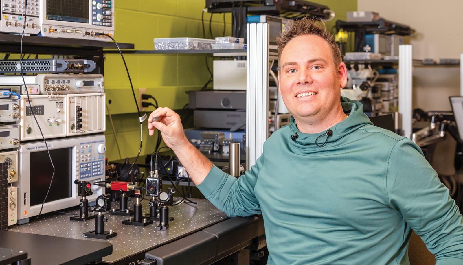
Back in 2010, when Engineering Professor Steve Adamshick was preparing to graduate with his Bachelor of Science in Electrical Engineering at WNE, he had no idea that the technology he regularly worked with — circuits, interferometers, and semiconductors — would soon be miniaturized into a silicon photonics platform. Now, he’s preparing the latest generation of engineers to continue pushing the bounds of innovation with his special topics course on silicon photonics. For the non-engineers: what, exactly, is silicon photonics?
Let’s break this down: silicon photonics is the creation of light circuits on a silicon-based platform.
Silicon, which is essentially sand and dirt melted down into particles, is the base material for what powers our digital existence: computer chips, central processing units (CPUs), and virtually all modern electronics. Silicon is also a base component of photovoltaic cells, or solar cells, which convert sunlight directly into energy. Those solar panels your neighbor installed last year — silicon! As silicon is one of the most abundant materials on Earth, it’s interesting to note that the dirt beneath our shoes transforms into computer chips that sell for thousands. Optics, or how we work with light, can be conceptualized with your hand-held camera. When you focus light on a subject or manipulate a shadow, you’re working with optics. Add geometric structures and fiber cables to the mix, and you’ve got fiber optics — transmission of light through a thread of glass or plastic. Shine a light into one end of a fiber optic cable, and it reaches the other end intact. Similarly, when encoded information such as internet and television data enters one end of a fiber optic cable, it’s converted back to its original form when it reaches the other side.
Photonics, or the manipulation of light, powers telecommunications, biosensing, environmental sensing, and — more recently — quantum computing.
When Professor Adamshick first taught the special topics course on silicon photonics in 2016, he focused on fundamentals, simulation, and mathematical problems. “There wasn’t a lot of hands-on to it,” he said.
Then, with a grant from the Massachusetts Center for Advanced Manufacturing and the Massachusetts Manufacturing Innovation Initiative, the College of Engineering gained a state-of-the-art optics/photonics training center known as the Laboratory for Education and Application Prototypes, or LEAP lab. Referred to as LEAP@WNE, the lab includes six instrumentation and prototyping workstations for students to apply the fundamentals of silicon photonics hands-on.
LEAP in Action
Professor Adamshick takes an inquisitive approach when guiding his students in chip design, asking questions like, “How do you build a setup? How do you envision that working? What are the core pieces of equipment that you need to get that done? Can you do that at scale?”
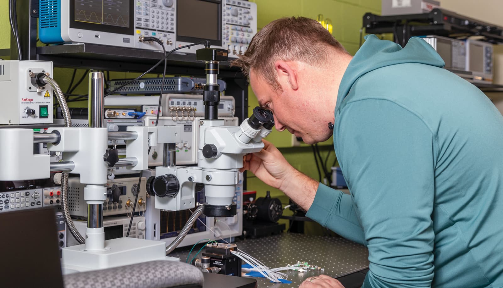
With no more than two students at any one of the six LEAP lab stations, each student has ample opportunity to create their own nanostructures that manipulate light on a computer chip. Once the chip is designed, it’s sent out to a manufacturer for fabrication. When students receive the fabricated chip, they are able to test it in the lab.
“Our students get to see that whole process as a closed loop, from the initial concept to how to implement the design of it,” Adamshick said.
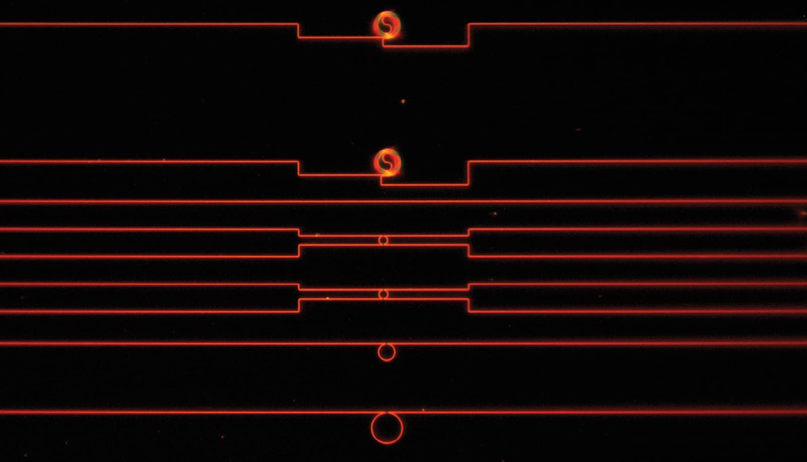
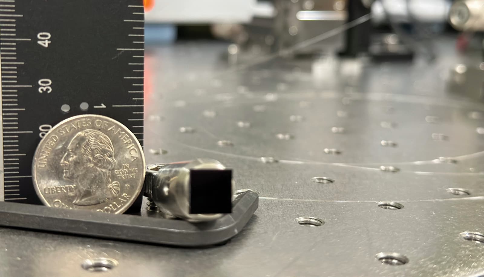
Ths chip image, codesigned by Electrical Engineering alumni Jacob Boisvere ’22 and Joseph Gonzalez ’22, was the first WNE chip design sent out for manufacturing. Boisvere and Gonzalez created the chip in the LEAP lab to study the coupling effects of ring resonator circuits, and the pair presented their results in the 2022 WNE Engineering Design Expo.
“The new equipment allowed me to engage deeply with the material outside of classroom lectures, and I frequently spent my time between classes experimenting with various devices and techniques … this practical approach became essential in helping me complete my senior project,” Gonzalez said.
In layman’s terms, Boisvere and Gonzalez examined how the electromagnetic field of one ring effected other nearby rings when a signal passed through. When designing efficient circuits, electrical engineers need to consider how this coupling effect strengthens or weakens signals passing through circuits. The rings are used in Wavelength Division Multiplexing communication schemes, which we typically associate with telecommunications companies. For example, if you’ve considered upgrading your Wi-Fi network to Fiber, you would essentially be combining multiple optical carrier signals into a single optical fiber.
Boisvere and Gonzalez were members of the first cohort to use the LEAP lab. Now a PhD candidate at Rochester Institute of Technology (RIT), Boisvere leverages his experience in developing the techniques for using LEAP lab equipment to further his research, which he has expanded to include optoelectronic and power devices in RIT’s Microsystems Engineering doctoral program.
“My experience with Dr. Adamshick has translated well to a research environment,” Boisvere said. “Much like my senior project, my work at RIT has been lab-focused and hands-on … I’ve co-authored publications on gallium nitride-based ultraviolet μLEDs and lasers, while working towards heterogeneous integration of these devices with silicon photonics through microtransfer printing.”
Known for his enthusiasm and passion for silicon photonics, Professor Adamshick introduces students to layout and simulation software in a project-based, hands-on environment. “Exploring the different applications, from Mach-Zehnder interferometers used to detect viral loads of COVID-19, to photonic ring resonators that allow specific wavelengths of light to be separated from many signals through a single fiber optic cable, allowed us to make real-world connections to the potentials of silicon photonics,” Boisvere explained.
K-12 STEM Outreach
WNE’s LEAP lab is one of five facilities in the state that houses application prototyping equipment. “What differentiates our lab from the others is that ours specifically focuses on workforce development,” Adamshick added.
And when it comes to workforce development, Adamshick recognizes the need to generate interest in the field. “The biggest shortage we have in our industry is human capital, and we’ve got to get students thinking STEM,” he said. In response, WNE partners with schools in the area to bring elementary- and secondary-age students into the lab.
Just like he does with his WNE students, Adamshick guides these younger groups with questions: “Do you want to use technology, or do you want to help make technology?” When students step into the LEAP lab at WNE, they can expect to see a live vibrometer demonstration on a silicon phonics platform and get their hands on photonic integrated circuit (PIC) chip kits created especially for K-12.
These PIC chip kits, developed by AIM Photonics in Albany, N.Y., and Spark Photonics in Waltham, Mass., were created specifically for educational and workforce development. WNE Engineering was the first customer of these kits designed and manufactured entirely in the U.S.
“In K-12 outreach, WNE has recognized the value of building a long-term pipeline of diverse STEM talent,” said Kevin McComber, CEO of Spark Photonics Design and executive director of Spark Photonics Foundation. “While many in higher education and industry focus intently on high school students nearing graduation, WNE has embraced the opportunity to reach students in middle school, where the data show many children decide whether to pursue STEM or non-STEM education and career pathways.”
At the nearby John J. Duggan Academy in Springfield, teachers and students in grades 6 through 12 engage in STEM programming through the partnership. “The collaboration between Spark Photonics and Western New England University has provided our students with real-world and hands-on activities to learn about the exciting career opportunities available in the field,” said Mary Kay Brown, Duggan’s director of partnerships.
The Future of Photonics
Of the first LEAP@WNE cohort, Joseph Gonzalez is now an electrical engineer with General Dynamics Mission Systems, where he works with schematic captures, investigates and troubleshoots schematics, and updates designs. Jacob Boisvere plans to “pursue academia after completion of [his] PhD, though there are some very interesting industry opportunities as the semiconductor industry within the United States continues to grow and develop.”
Regarding the K-12 STEM pipeline, Mary Kay Brown of Duggan Academy hopes to continue this collaboration so photonics can be a viable career pathway for students.
WNE will continue to make its mark on the global photonics community as host of the 67th International Midwest Symposium on Circuits and Systems this August. The symposium, sponsored by the Institute of Electrical and Electronics Engineers (IEEE), draws international experts in the areas of analog and digital circuits and systems. The theme for this year is “Driving the future of Integrated Microelectronics: Analog, Digital & Photonics to address global societal needs.”
Now that computer chip manufacture is completely automated, engineers have shifted their focus from assembly-line production to making components and machines that use artificial intelligence (AI) optimization. “Not only are we seeing innovation in silicon photonics, but we’re also seeing innovation in artificial learning and quantum computing — those technologies all rely on that core component trio,” Adamshick explained, referring to silicon.
“50 years ago, semiconductor manufacturing and innovation mostly happened right here in the US. However, 25 years ago, much of the semiconductor ecosystem left the US, and now recently there’s an emphasis to bring manufacturing and innovation back to the US,” Adamshick added. “These core systems have such a reliance on [silicon/semiconductor manufacturing], and we need to ensure that essential supply chain stays intact and that we can depend on it.”
Back in the LEAP lab, students from the most recent silicon photonics course created a biosensor on a silicon platform that detects COVID. This presents an opportunity for electrical and biomedical engineering students to collaborate on further developing the project — potentially as a senior design project for the upcoming academic year.
When it comes to projects that carry a seemingly infinite number of variables such as virus detection and vaccine development, silicon photonics offers a way of calculating all possible solutions through quantum computing. “Silicon photonics is also a key player in developing quantum computing architectures that can operate at room temperatures by delivering focused light to individual neutral atoms,” Adamshick explained. He added that “a lot of venture capitalism is going into these photonics solutions because we don’t need the infrastructure of a dilution refrigerator system as required for superconducting qubit-based quantum computing architectures, where materials are cooled to temperatures approaching absolute zero degrees Kelvin.”
Outside the lab, as a former student-athlete himself, Adamshick values the well-rounded student experience at WNE. “Coach Downes was instrumental in my decision-making process to pursue a degree at WNE, as it was really the only school that said yes, you can be a student-athlete and yes, you can complete your engineering degree,” he explained. “That’s important to students who grew up playing a sport and want to continue playing a sport.” Not only was Adamshick captain of the men’s golf team as a student, but he also met his wife, Kelly Coakley ’10/G’11 on campus.
“This place is like home,” Adamshick said of his alma mater and employer. And — beyond matters of the heart — home is where the innovation is.